Sony’s new image sensor could give far better dynamic vary and sounds reduction
At the IEEE Worldwide Electron Gadgets Assembly, Sony announced its most recent breakthrough in smartphone digicam technology. Sony unveiled the world’s initial stacked CMOS (Complementary Metal Oxide Semiconductor) graphic sensor with a dual-layer transistor pixel.
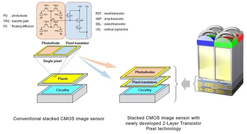
Sony’s dual CMOS picture sensor differs from conventional CMOS graphic sensors in that it has unbiased photodiodes and pixel transistors on different substrate layers. A CMOS impression sensor has a layered development that consists of a pixel chip with back-illuminated pixels stacked above a logic chip with sign processing circuits.
As opposed to classic CMOS impression sensors, which have photodiodes and pixel transistors on the identical substrate layer, Sony’s revolutionary technologies has photodiodes and pixel transistors on different substrate layers.
Sony’s new CMOS architecture know-how optimizes the photodiode and the pixel transistor levels by doubling the saturation signal amount and widening the dynamic range of an image. As a consequence, the imaging qualities are significantly improved. The new pixel composition will enable pixels to manage or improve their current properties at the two latest and minimized pixel sizes.The new CMOS design permits Sony to maximize the sizing of the amplifier transistors. With the enhanced dimensions, Sony lowers the total of sounds that nighttime and other dim-locale shots could have.
Sony’s new CMOS technological know-how will avert underexposure and overexposure in situations with mixed lights. Its most current image sensor style and design is promised to make it possible for substantial-top quality, small-noise pics even in low-mild conditions.
Sony reported that its new CMOS technological know-how is intended for smartphones but did not provide a time body when we could be expecting to obtain phones employing this new sensor style and design.


